| CPC H01L 23/528 (2013.01) [H01L 23/5226 (2013.01); H01L 29/0649 (2013.01)] | 20 Claims |
|
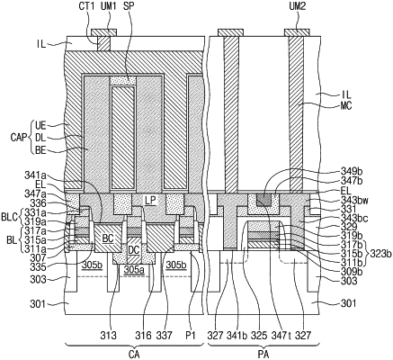
1. A semiconductor device, comprising:
a substrate including a cell region and a peripheral region around the cell region;
a bit line structure on the cell region of the substrate, the bit line structure including a first side and a second side opposite the first side;
a first cell contact adjacent to the first side of the bit line structure;
a second cell contact adjacent to the second side of the bit line structure;
a cell contact separation pattern between the first cell contact and the second cell contact;
a peripheral gate structure on the peripheral region of the substrate, the peripheral gate structure including a first side and a second side opposite the first side;
a first interlayer insulating layer covering the peripheral gate structure;
a second interlayer insulating layer on the first interlayer insulating layer;
a first peripheral contact arranged adjacent to the first side of the peripheral gate structure and penetrating the first and second interlayer insulating layers;
a second peripheral contact arranged adjacent to the second side of the peripheral gate structure and penetrating the first and second interlayer insulating layers; and
a peripheral contact separation pattern between the first peripheral contact and the second peripheral contact,
wherein the peripheral contact separation pattern includes:
a first peripheral contact separation pattern having a trench that is defined by a first side surface, a second side surface opposite the first side surface, and a bottom surface between the first side surface and the second side surface; and
a second peripheral contact separation pattern filling the trench of the first peripheral contact separation pattern,
wherein the second peripheral contact separation pattern includes a concave top surface that is higher than a top surface of the second interlayer insulating layer, and
wherein a bottom surface of the second peripheral contact separation pattern is lower than the top surface of the second interlayer insulating layer.
|