| CPC H01L 23/528 (2013.01) [H01L 24/05 (2013.01); H01L 24/13 (2013.01); H01L 24/26 (2013.01); H01L 25/0655 (2013.01); H01L 2224/0401 (2013.01); H01L 2224/13026 (2013.01); H01L 2224/16227 (2013.01)] | 20 Claims |
|
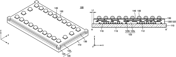
1. A semiconductor device comprising:
a semiconductor substrate having a semiconductor device on an active surface thereof, the semiconductor substrate having a quadrangular plane;
an insulating layer disposed directly on the active surface of the semiconductor substrate; and
a passivation layer on the insulating layer,
wherein the insulating layer includes:
an insulating layer central portion having a side surface extending in parallel with a side surface of the semiconductor substrate, the side surface of the insulating layer central portion is spaced apart from the side surface of the semiconductor substrate by a first size; and
an insulating layer corner portion at each corner of the insulating layer central portion and protruding from the side surface of the insulating layer central portion in a horizontal direction, and
the passivation layer covers the insulating layer central portion.
|