| CPC H01L 23/528 (2013.01) [H01L 23/3171 (2013.01); H01L 24/03 (2013.01); H01L 24/05 (2013.01); H01L 2224/02311 (2013.01); H01L 2224/02313 (2013.01); H01L 2224/02373 (2013.01); H01L 2224/0401 (2013.01)] | 20 Claims |
|
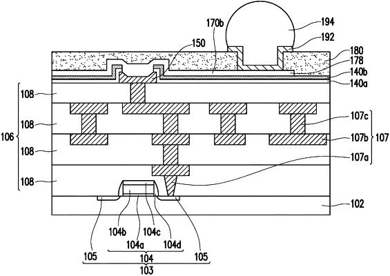
1. A semiconductor device, comprising:
a semiconductor substrate, comprising a conductive pad thereover;
a passivation layer over the semiconductor substrate;
a post-passivation interconnect (PPI) structure, disposed over the passivation layer and electrically connected to the conductive pad, wherein the PPI structure comprises a first portion including a first sidewall, a second sidewall and a bottom, the second sidewall is disposed between the first sidewall and the bottom, a first angle formed between the first sidewall and the second sidewall is an obtuse angle, and a second angle formed between the second sidewall and the bottom is an obtuse angle, wherein part of the first portion is partially embedded in the conductive pad; and
a conductive terminal, disposed over and electrically connected to the PPI structure.
|