| CPC H01L 23/5226 (2013.01) [H01L 21/28568 (2013.01); H01L 21/76802 (2013.01); H01L 21/76843 (2013.01); H01L 21/76864 (2013.01); H01L 21/76877 (2013.01); H01L 23/528 (2013.01); H01L 23/53266 (2013.01)] | 20 Claims |
|
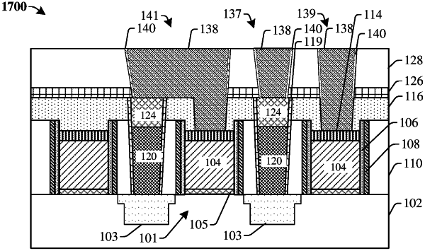
1. A method of manufacturing an integrated circuit device, comprising:
forming a lower inter-layer dielectric (ILD) layer over a substrate;
forming a lower conductive plug through the lower ILD layer on a source/drain region of a transistor structure;
forming a capping layer on the lower conductive plug;
forming an upper ILD layer over the lower ILD layer and the capping layer; and
forming an upper conductive plug through the upper ILD layer reaching the capping layer;
wherein the upper conductive plug is formed by forming a metal core followed by an annealing process to form an intermixing barrier layer lining an interface of the metal core and the upper ILD layer.
|