| CPC H01L 23/49838 (2013.01) [H01L 21/4853 (2013.01); H01L 21/4857 (2013.01); H01L 21/486 (2013.01); H01L 23/13 (2013.01); H01L 23/49822 (2013.01); H01L 23/49827 (2013.01); H01L 23/5389 (2013.01); H01L 25/16 (2013.01); H01L 23/3128 (2013.01); H01L 23/50 (2013.01); H01L 24/13 (2013.01); H01L 24/16 (2013.01); H01L 25/0655 (2013.01); H01L 2224/0401 (2013.01); H01L 2224/131 (2013.01); H01L 2224/13147 (2013.01); H01L 2224/16227 (2013.01); H01L 2224/16235 (2013.01); H01L 2224/16237 (2013.01); H01L 2924/1432 (2013.01); H01L 2924/1434 (2013.01); H01L 2924/15159 (2013.01); H01L 2924/19041 (2013.01); H01L 2924/19042 (2013.01); H01L 2924/19043 (2013.01); H01L 2924/19103 (2013.01); H01L 2924/19106 (2013.01)] | 20 Claims |
|
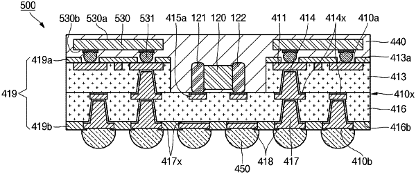
1. A semiconductor package comprising:
a substrate comprising:
a first substrate surface;
a second substrate surface opposite the first substrate surface;
a recess portion in the first substrate surface and extending toward the second substrate surface;
a plurality of recess conductive patterns in the recess portion;
a dielectric layer having a first dielectric surface, a second dielectric surface, and a side dielectric surface extending between the first dielectric surface and the second dielectric surface, wherein the recess portion extends from the first dielectric surface to the second dielectric surface adjacent the side dielectric surface;
a first conductive pattern at the first dielectric surface;
a second conductive pattern at the second dielectric surface; and
a conductive via that passes through the dielectric layer and electrically connects the first conductive pattern and the second conductive pattern;
a passive element positioned in the recess portion of the substrate and comprising a first electrode and a second electrode, each electrically connected to a respective pattern of the plurality of recess conductive patterns;
a semiconductor die mounted on the first dielectric surface and connected to the first conductive pattern;
a layer of a single continuous encapsulating material that contacts the side dielectric surface, covers at least a first side and lateral sides of the passive element, covers at least a portion of the first substrate surface, and covers at least lateral sides of the semiconductor die and a first side of the semiconductor die facing away from the dielectric layer.
|