| CPC H01L 23/49822 (2013.01) [H01L 23/3128 (2013.01); H01L 23/5386 (2013.01); H01L 23/5389 (2013.01); H01L 24/16 (2013.01); H01L 25/105 (2013.01); H01L 2224/16227 (2013.01)] | 19 Claims |
|
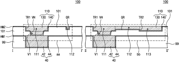
1. An interconnection structure, comprising:
a first dielectric layer and a first hardmask pattern that are sequentially stacked; and
a first interconnection pattern that penetrates the first hardmask pattern and the first dielectric layer, wherein
the first hardmask pattern includes a dielectric material having an etch selectivity with respect to the first dielectric layer,
the first interconnection pattern includes a via part, a first pad part, and a line part that are integrally connected to each other,
the first pad part vertically overlapping the via part,
the line part extends from the first pad part,
a level of a bottom surface of the first pad part is lower than a level of a bottom surface of the line part,
a top surface of the first pad part and a top surface of the line part are coplanar with a top surface of the first hardmask pattern, and
the bottom surface of the first pad part, the bottom surface of the line part, and a lateral surface of the via part are in contact with the first dielectric layer.
|