| CPC H01L 23/49541 (2013.01) [H01L 23/3178 (2013.01); H01L 23/481 (2013.01)] | 15 Claims |
|
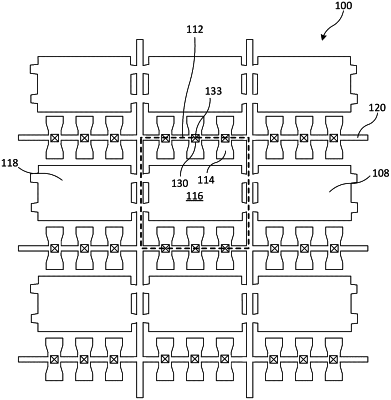
1. A method of forming a packaged semiconductor device, comprising:
providing a leadframe blank including a first package blank, a second package blank and a tie bar between the first package blank and the second package blank, each package blank comprising a die attach pad and a lead, wherein the leads of the first and second package blanks are attached to the tie bar;
forming a recessed cavity in the tie bar; and
separating the first and second package blanks along the tie bar,
wherein each package blank comprises a plurality of leads attached to the tie bar at respective attachment points, the method further comprising forming a plurality of recessed cavities in the tie bar at the attachment points.
|