| CPC H01L 23/3675 (2013.01) [H01L 21/4871 (2013.01); H01L 21/6835 (2013.01); H01L 21/78 (2013.01); H01L 24/16 (2013.01); H01L 25/0655 (2013.01); H01L 25/18 (2013.01); H01L 25/50 (2013.01); H01L 2221/68331 (2013.01); H01L 2224/16225 (2013.01); H01L 2924/1431 (2013.01); H01L 2924/1434 (2013.01)] | 20 Claims |
|
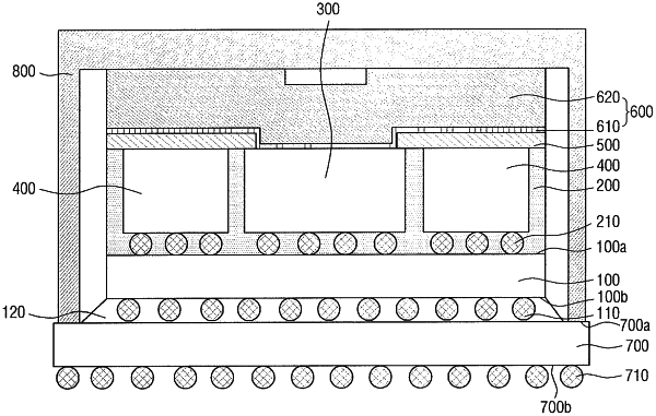
1. A semiconductor package, comprising:
a first semiconductor chip and a second semiconductor chip on a substrate, the first and second semiconductor chips being equal in thickness such that uppermost faces of the first and second semiconductor chips are located at a same height from the substrate;
a barrier layer having an opening that exposes a first portion of the uppermost face of the first semiconductor chip, the barrier layer being in contact with a second portion of the uppermost face of the first semiconductor chip not exposed by the opening and an entirety of the uppermost face of the second semiconductor chip and; and
a heat transfer part on the barrier layer, the heat transfer part extending along an upper face of the barrier layer and filling the opening.
|