| CPC H01L 23/367 (2013.01) [H01L 23/3128 (2013.01); H01L 23/49822 (2013.01); H01L 24/16 (2013.01); H01L 24/32 (2013.01); H01L 24/73 (2013.01); H01L 25/16 (2013.01); H01L 2224/16227 (2013.01); H01L 2224/32225 (2013.01); H01L 2224/73204 (2013.01)] | 19 Claims |
|
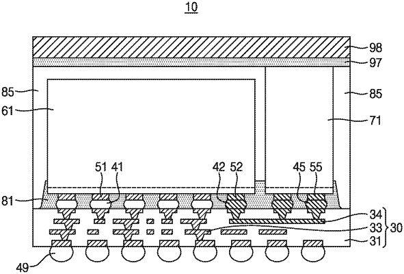
1. A semiconductor package comprising:
a wiring structure including signal wiring and a heat transfer wiring spaced apart from the signal wiring;
an active chip on the wiring structure;
a signal terminal disposed between the wiring structure and the active chip;
a first heat transferring terminal disposed between the wiring structure and the active chip and connected to the heat transfer wiring;
a passive chip on the wiring structure;
a second heat transferring terminal disposed between the wiring structure and the passive chip and connected to the heat transfer wiring; and
a heat spreader on the passive chip,
wherein the passive chip is an electrically inactive dummy chip, and
wherein the heat transfer wiring is a single wiring in the wiring structure, and the plurality of first heat transferring terminals and the plurality of second heat transferring terminals are commonly connected to the single wiring.
|