| CPC H01L 23/16 (2013.01) [H01L 23/3185 (2013.01); H01L 23/49822 (2013.01); H01L 23/49838 (2013.01); H01L 24/16 (2013.01); H01L 25/0655 (2013.01); H01L 2224/16227 (2013.01); H01L 2924/18161 (2013.01)] | 26 Claims |
|
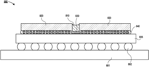
1. An electronic package, comprising:
a package substrate;
a plurality of interconnects on the package substrate;
a die coupled to the package substrate by the plurality of interconnects, the die having a footprint;
a flow control feature on the package substrate, wherein the flow control feature is electrically isolated from circuitry of the electronic package, wherein the flow control feature comprises a plurality of substantially parallel lines, and wherein the flow control feature is continuous from a location within the footprint of the die to a location outside of the footprint of the die; and
an underfill surrounding the plurality of interconnects and in contact with the flow control feature.
|