US 12,009,270 B2
Welding method of demetallized ceramic substrate having surface capillary microgroove structure
Zongtao Li, Guangzhou (CN); Yong Tang, Guangzhou (CN); Hong Wang, Guangzhou (CN); Shudong Yu, Guangzhou (CN); Kejian Wu, Guangzhou (CN); Guanwei Liang, Guangzhou (CN); and Xinrui Ding, Guangzhou (CN)
Assigned to SOUTH CHINA UNIVERSITY OF TECHNOLOGY, Guangzhou (CN); GUANGDONG LUCKYSTAR ELECTRONIC TECHNOLOGY CO., LTD, Guangdong (CN); and SHENZHEN GOOD-MACHINE AUTOMATIC EQUIPMENT CO., LTD, Guangdong (CN)
Appl. No. 17/607,901
Filed by SOUTH CHINA UNIVERSITY OF TECHNOLOGY, Guangzhou (CN); GUANGDONG LUCKYSTAR ELECTRONIC TECHNOLOGY CO., LTD, Guangdong (CN); and SHENZHEN GOOD-MACHINE AUTOMATIC EQUIPMENT CO., LTD, Guangdong (CN)
PCT Filed Nov. 14, 2019, PCT No. PCT/CN2019/118291
§ 371(c)(1), (2) Date Nov. 1, 2021,
PCT Pub. No. WO2020/220643, PCT Pub. Date Nov. 5, 2020.
Claims priority of application No. 201910364622.5 (CN), filed on Apr. 30, 2019.
Prior Publication US 2022/0293480 A1, Sep. 15, 2022
Int. Cl. H01L 23/13 (2006.01); H01L 23/15 (2006.01); H01L 33/62 (2010.01)
CPC H01L 23/13 (2013.01) [H01L 23/15 (2013.01); H01L 33/62 (2013.01)] 9 Claims
OG exemplary drawing
 
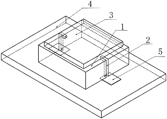
1. A welding method of a demetallized ceramic substrate having a surface capillary microgroove structure, the demetallized ceramic substrate comprising a ceramic substrate main body and surface capillary microstructures, the surface capillary microstructures being arranged on two lateral sides of the ceramic substrate main body and the surface capillary microstructures specifically being capillary microgrooves, the welding method comprises the following steps:
Step (1) fixing a chip to an upper surface of the demetallized ceramic substrate having the surface capillary microgroove structure;
Step (2) fixing the demetallized ceramic substrate with the chip to a printed circuit board having a bonding pad; and
Step (3) placing melted solder on the bonding pad, and driving the melted solder to ascend to an electrode of the chip from the bonding pad in a lower layer by means of a capillary force, thereby realizing an electrical connection between the chip and the printed circuit board.