| CPC H01L 22/12 (2013.01) [H01L 21/221 (2013.01); H01L 21/265 (2013.01); H01L 21/26526 (2013.01); H01L 21/324 (2013.01); H01L 27/0664 (2013.01); H01L 29/0611 (2013.01); H01L 29/0615 (2013.01); H01L 29/0619 (2013.01); H01L 29/0623 (2013.01); H01L 29/1095 (2013.01); H01L 29/32 (2013.01); H01L 29/407 (2013.01); H01L 29/7397 (2013.01); H01L 29/8613 (2013.01)] | 20 Claims |
|
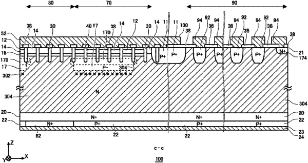
1. A semiconductor device comprising:
a plurality of trench portions arrayed in a first direction on an upper surface side of a semiconductor substrate;
a first lower surface region of a first conductivity type provided in at least a part of a lower surface of the semiconductor substrate;
a base region of a second conductivity type provided on the upper surface side of the semiconductor substrate;
a first region of the first conductivity type provided in the semiconductor substrate and disposed between the base region and the first lower surface region in a depth direction of the semiconductor substrate;
a first upper surface region of the first conductivity type provided on an upper surface of the semiconductor substrate; and
a first bottom region of the second conductivity type provided in the semiconductor substrate and disposed continuously in the first direction such that the first bottom region is in contact with bottom portions of the plurality of trench portions, wherein
in a cross section that (i) is along the first direction and perpendicular to the upper surface and the lower surface of the semiconductor substrate and (ii) passes through the first lower surface region, one end portion of the first bottom region in the first direction locates directly above the first lower surface region in the depth direction.
|