| CPC H01L 21/823481 (2013.01) [H01L 21/76224 (2013.01); H01L 21/764 (2013.01); H01L 21/823437 (2013.01); H01L 27/0886 (2013.01); H01L 21/02164 (2013.01); H01L 21/0217 (2013.01); H01L 21/02274 (2013.01); H01L 21/0228 (2013.01)] | 20 Claims |
|
1. A method, comprising:
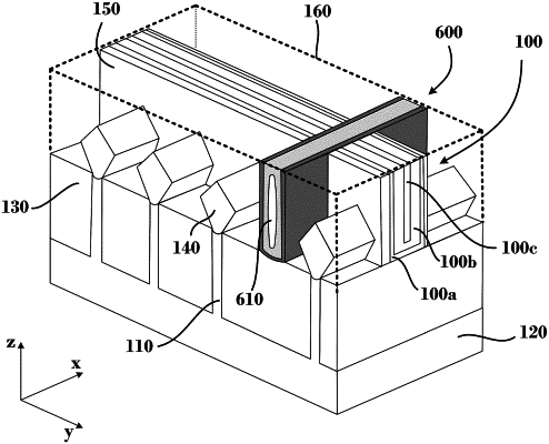
forming a gate structure on fin structures disposed on a substrate;
forming an opening of substantially constant width in the gate structure between two adjacent fin structures, to divide the gate structure into first and second sections spaced apart by the opening, wherein the opening has a height to width ratio of about 8:1, the width being in a direction perpendicular to a length of the fin structures and parallel to the substrate, and wherein forming the opening comprises forming a recess in a dielectric layer between the fin structures;
depositing a silicon nitride liner in the opening to cover sidewall surfaces of the opening; and
depositing a silicon oxide fill layer in the opening and on the silicon nitride liner, comprising forming an air gap within the silicon oxide fill layer.
|