| CPC H01L 21/823412 (2013.01) [H01L 21/823418 (2013.01); H01L 21/823431 (2013.01); H01L 27/0886 (2013.01); H01L 29/0665 (2013.01); H01L 29/42392 (2013.01); H01L 29/66545 (2013.01); H01L 29/78618 (2013.01); H01L 29/78696 (2013.01)] | 20 Claims |
|
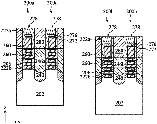
10. A semiconductor structure, comprising:
a first fin structure including a first stack of active channel layers and protruding from a substrate;
a second fin structure including a second stack of active channel layers disposed over at least one dummy channel layer and protruding from the substrate;
a gate structure engaged with the first stack and the second stack;
a first source/drain (S/D) feature disposed in the first fin structure and adjacent to the first stack, wherein the first S/D feature includes a first doped epitaxial layer over an un-doped epitaxial layer; and
a second S/D feature disposed in the second fin structure and adjacent to the second stack, wherein the second S/D feature includes a second doped epitaxial layer over the un-doped epitaxial layer, and wherein the un-doped epitaxial layer overlaps with the at least one dummy channel layer.
|