| CPC H01L 21/76895 (2013.01) [H01L 21/76805 (2013.01); H01L 21/76816 (2013.01); H01L 21/76831 (2013.01); H01L 23/528 (2013.01); H01L 23/535 (2013.01); H01L 29/66545 (2013.01); H01L 29/66636 (2013.01); H01L 29/7848 (2013.01); H01L 29/0847 (2013.01); H01L 29/165 (2013.01)] | 20 Claims |
|
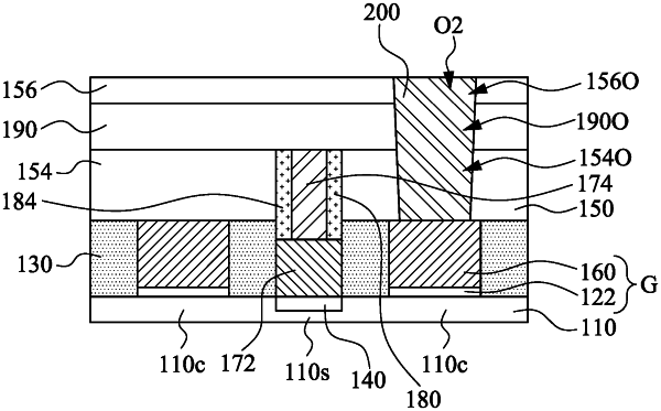
1. A semiconductor device, comprising:
a semiconductor substrate having a channel region and a source/drain region;
a gate electrode over the channel region;
a source/drain contact over the source/drain region;
a conductive structure over a top surface of the source/drain contact;
an interlayer dielectric (ILD) layer surrounding the conductive structure and over the gate electrode;
an etch stop layer over the conductive structure and the ILD layer, wherein the etch stop layer comprises a material different from that of the ILD layer, and a top surface of the conductive structure is in contact with a bottom surface of the etch stop layer;
a dielectric liner at a sidewall of the conductive structure, wherein the dielectric liner extends from the top surface of the source/drain contact to the bottom surface of the etch stop layer; and
a gate contact over the gate electrode, wherein a top surface of the gate contact is higher than a top surface of the etch stop layer.
|