| CPC H01L 21/76835 (2013.01) [H01L 21/0228 (2013.01); H01L 21/02304 (2013.01); H01L 21/31144 (2013.01); H01L 21/76802 (2013.01); H01L 21/76837 (2013.01); H01L 21/76877 (2013.01); H01L 21/823475 (2013.01); H01L 23/5283 (2013.01); H01L 23/53295 (2013.01); H01L 27/0886 (2013.01); H01L 29/41791 (2013.01); H01L 29/4232 (2013.01)] | 20 Claims |
|
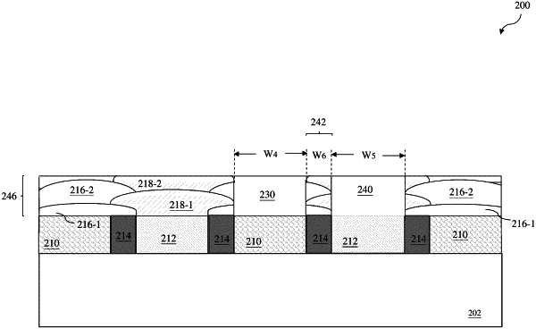
1. A semiconductor structure, comprising:
a semiconductor substrate;
a first via feature and a second via feature disposed on the semiconductor substrate; and
a staggered dielectric feature interposed between the first and second via features, wherein
the staggered dielectric feature includes a plurality of first dielectric layers and a plurality of second dielectric layers being interdigitated,
the first dielectric layers include a first dielectric material and the second dielectric layers include a second dielectric material being different from the first dielectric material, and
each of the first dielectric layers and each of the second dielectric layers continuously extends from the first via feature to the second via feature, and contacts both the first and second via features.
|