| CPC H01L 21/68757 (2013.01) [C23C 16/24 (2013.01); H01J 37/32477 (2013.01); H01J 37/32715 (2013.01); H01L 21/311 (2013.01); H01L 21/31116 (2013.01); H01L 21/68735 (2013.01)] | 9 Claims |
|
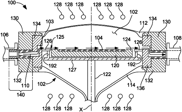
1. A method for etching semiconductor structures in a processing reactor comprising a susceptor which supports a semiconductor structure within a recess of the susceptor, the method comprising:
depositing a first polycrystalline silicon surface layer on the susceptor at a temperature of less than 1150° C.;
loading a first semiconductor structure onto the susceptor having the first polycrystalline silicon surface layer disposed thereon, the first semiconductor structure being disposed within the recess;
contacting the first semiconductor structure with an etchant to etch the semiconductor structure, the first semiconductor structure that is etched being the first semiconductor structure loaded onto the susceptor after the first polycrystalline silicon surface layer is deposited on the susceptor;
removing the first semiconductor structure from the susceptor after the first semiconductor structure has been etched;
contacting the susceptor with a stripping etchant to strip the first polycrystalline silicon surface layer from the susceptor;
depositing a second polycrystalline silicon surface layer on the susceptor at a temperature of less than 1150° C.;
loading a second semiconductor structure onto the susceptor having the second polycrystalline silicon surface layer disposed thereon, the first and second semiconductor structures being semiconductor structures that are consecutively loaded onto the susceptor; and
contacting the second semiconductor structure with the etchant to etch the second semiconductor structure.
|