| CPC H01L 21/67772 (2013.01) [B65G 47/90 (2013.01); H01L 21/67373 (2013.01); H01L 21/67376 (2013.01); H01L 21/67766 (2013.01)] | 20 Claims |
|
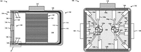
1. A wafer transport container, comprising:
a housing, comprising:
a shell forming an internal space that is configured to hold a plurality of wafers;
an opening configured to provide access to the internal space; and
a first pair of magnets and a second pair of magnets that are positioned around a perimeter of the opening of the housing; and
a door configured to form an air-tight seal around the perimeter of the opening, comprising:
a third pair of magnets and a fourth pair of magnets that are positioned around a perimeter of the door,
wherein the third pair of magnets is configured to interface with the first pair of magnets, and
wherein the fourth pair of magnets is configured to interface with the second pair of magnets;
a first latch;
a second latch;
a first support member connected to the first latch and a magnet of the third pair of magnets; and
a second support member connected to the second latch and the magnet.
|