| CPC H01L 21/486 (2013.01) [H01L 23/49827 (2013.01); H01L 23/15 (2013.01)] | 10 Claims |
|
1. An electrical component comprising:
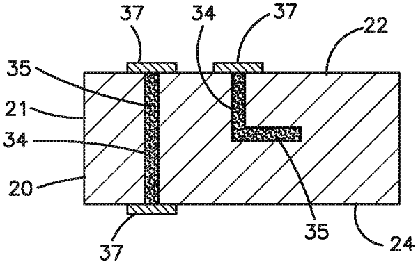
a substrate defining a first surface and a second surface opposite the first surface, and a hole that extends from the first surface to the second surface; and
an electrically conductive metal fill that extends in the hole from the first surface to the second surface so as to define an electrically conductive via, wherein the electrically conductive fill defines an electrically conductive path from the first surface to the second surface,
wherein the metal fill comprises sintered metal particles, and a majority of the metal particles are substantially non-densification sintered, and
wherein respective geometric centers of adjacent substantially non-densification sintered metal particles are spaced apart a distance that defines a difference with respect a distance between the geometric centers prior to sintering, and the difference is no more than 30% of the distance between the geometric centers prior to sintering.
|