| CPC H01L 21/3212 (2013.01) [H01L 21/02074 (2013.01); H01L 21/0228 (2013.01); H01L 21/28 (2013.01); H01L 21/302 (2013.01); H01L 21/32139 (2013.01); H01L 21/67046 (2013.01); H01L 21/67051 (2013.01); H01L 21/76829 (2013.01)] | 20 Claims |
|
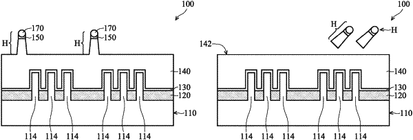
1. A method for forming a semiconductor device structure, comprising:
forming a first layer over a substrate;
forming a stop layer over the first layer;
forming a second layer over the stop layer, wherein the second layer is in direct contact with the stop layer;
partially removing the second layer;
performing an etching process to partially remove the stop layer and an upper portion of the first layer, wherein protrusion structures are formed over a lower portion of the first layer after the etching process, and the protrusion structures comprise the stop layer and the upper portion of the first layer remaining after the etching process; and
removing the protrusion structures.
|