| CPC H01L 21/3212 (2013.01) [G01N 23/20075 (2013.01); G06F 11/07 (2013.01); H01L 22/26 (2013.01); B24B 37/013 (2013.01); G01N 1/10 (2013.01)] | 20 Claims |
|
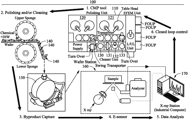
1. A system, comprising:
a chemical-mechanical-polishing (CMP) tool configured to polish a wafer, wherein a polishing of the wafer generates byproducts;
a byproduct-collection tool configured to collect at least some of the byproducts generated during the polishing of the wafer;
a sensor, an analyzer, and first computer configured to analyze the collected byproducts, wherein an analysis of the collected byproducts indicates:
a presence of an unexpected atomic element that corresponds to a contaminant material in the collected byproducts; or
an unexpected chronological sequence in which a plurality of atomic elements in the collected byproducts appear; and
an industrial-grade computer configured to instruct the CMP tool to adjust the polishing of the wafer based on the analysis of the collected byproducts indicating an error that includes a contamination of the CMP tool, an over-polishing of the wafer, or an under-polishing of the wafer.
|