| CPC H01L 21/28518 (2013.01) [H01L 21/764 (2013.01); H01L 29/0653 (2013.01); H01L 29/45 (2013.01); H01L 29/6653 (2013.01); H01L 29/66795 (2013.01); H01L 29/7851 (2013.01); H01L 2029/7858 (2013.01)] | 20 Claims |
|
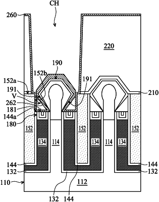
1. A semiconductor device structure, comprising:
a substrate having a base portion and a fin portion over the base portion;
an epitaxial structure over the fin portion;
a dielectric fin over the base portion; and
a silicide layer between the dielectric fin and the epitaxial structure, wherein a void is between the silicide layer and the dielectric fin.
|