| CPC H01L 21/0338 (2013.01) [H01L 21/02255 (2013.01); H01L 21/02271 (2013.01); H01L 21/0332 (2013.01); H01L 21/0335 (2013.01); H01L 21/0337 (2013.01); H01L 21/31155 (2013.01)] | 11 Claims |
|
1. A semiconductor structure, comprising:
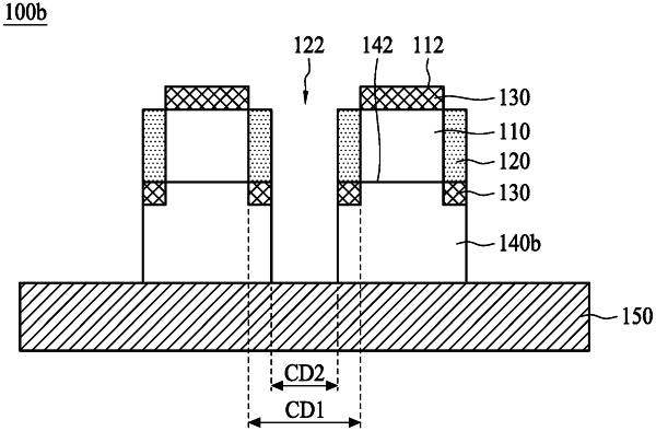
a base layer with a top surface;
a primary pattern with a pattern top surface and a sidewall, disposed on the top surface of the base layer, wherein the primary pattern has a first critical dimension;
a plurality of first ion implantation layers formed on the pattern top surface and a plurality of second ion implantation layers formed on a part of the top surface of the base layer exposed by the primary pattern, wherein the first ion implantation layers and the second implantation layers form a plurality of processed areas on the pattern top surface and the part of the top surface of the base layer exposed by the primary pattern, wherein the first ion implantation layers and the second implantation layers have no contact with each other; and
a secondary pattern disposed on the sidewall of the primary pattern, wherein the secondary pattern has a second critical dimension, and the second critical dimension is smaller than the first critical dimension, wherein the secondary pattern has no contact with the first ion implantation layers while the secondary pattern is direct contact with at least one of the second implantation layers.
|