| CPC H01L 21/02658 (2013.01) [C23C 16/24 (2013.01); C23C 16/26 (2013.01); C23C 16/4404 (2013.01); C23C 16/4405 (2013.01); H01L 21/02238 (2013.01)] | 18 Claims |
|
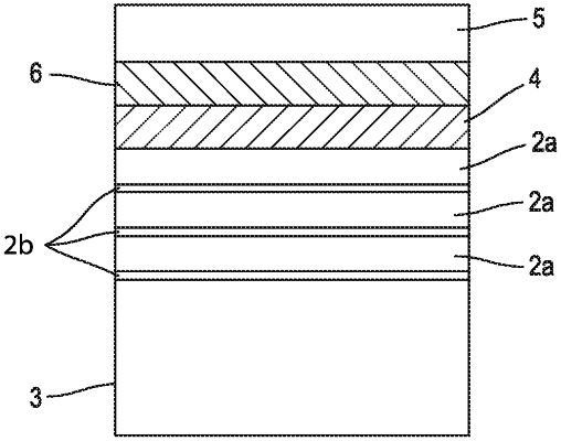
1. A charge trapping layer for a semiconductor structure support, comprising:
at least one polycrystalline charge trapping material; and
at least one polycrystalline interlayer directly adjacent to the charge trapping material, the at least one polycrystalline interlayer comprising an alloy of silicon and carbon,
wherein a lattice parameter of the at least one polycrystalline charge trapping material is greater than a lattice parameter of the at least one polycrystalline interlayer.
|