| CPC H01L 21/0254 (2013.01) [H01L 21/746 (2013.01); H01L 29/205 (2013.01); H01L 29/404 (2013.01); H01L 29/407 (2013.01); H01L 29/66462 (2013.01); H01L 29/778 (2013.01); H01L 29/7786 (2013.01); H01L 29/2003 (2013.01)] | 16 Claims |
|
1. A method of manufacturing a semiconductor device, the method comprising:
receiving, obtaining, or providing a starting material that comprises:
a first substrate having a first crystal structure,
a layer of sacrificial material that has a second crystal structure based on the first crystal structure and is adjacent to the first substrate,
a first portion of a layer of a first semiconducting material that has a third crystal structure based on the first crystal structure and is adjacent to the layer of sacrificial material,
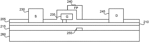
a layer of etch stop material on the first portion of the layer of the first semiconducting material,
growing a second portion of the layer of the first semiconducting material over the first portion of the layer of the first semiconducting material and the layer of etch stop material, the second portion having a specified height, wherein the etch stop material and the specified height are selected to determine a distance of a backside field plate formed in the layer of the first semiconducting material from a heterojunction, and
a layer of a second semiconducting material that forms the heterojunction with the layer of the first semiconducting material;
forming a first component of the semiconductor device, the first component electrically coupled to the heterojunction; and
removing the first substrate to expose a surface of the layer of the first semiconducting material.
|