| CPC H01L 21/02304 (2013.01) [H01L 21/76802 (2013.01); H01L 21/76877 (2013.01); H01L 23/5222 (2013.01); H01L 23/5226 (2013.01)] | 20 Claims |

|
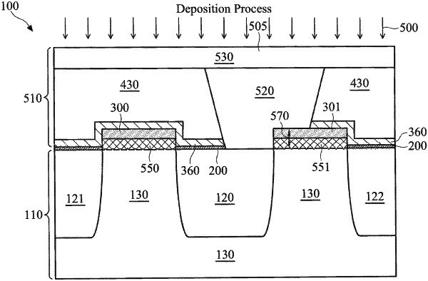
1. A method, comprising:
providing a structure that includes a first conductive component and a first interlayer dielectric (ILD) that surrounds the first conductive component;
selectively forming a self-assembly layer directly on an upper surface of the first conductive component;
selectively forming a first dielectric layer over the first ILD;
forming a second ILD over the first conductive component and over the first ILD;
etching an opening in the second ILD, wherein the opening is at least partially aligned with the first conductive component, wherein the first dielectric layer protects portions of the first ILD located therebelow from being etched; and
filling the opening with a conductive material to form a second conductive component in the opening.
|