| CPC H01J 37/32972 (2013.01) [G01B 11/0625 (2013.01); G01B 11/0683 (2013.01); H01J 37/32467 (2013.01); H01J 37/32862 (2013.01); H01J 37/32963 (2013.01); H01L 22/26 (2013.01); H01J 2237/24585 (2013.01); H01J 2237/332 (2013.01)] | 19 Claims |

|
1. A system comprising:
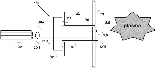
a transparent crystal, wherein at least part of the transparent crystal is embedded within a wall and a liner of a processing chamber;
a transparent thin film deposited on a surface of the transparent crystal that is exposed to an interior of the processing chamber;
a spectrometer configured to:
receive light reflected from a surface of the transparent thin film and a surface of a process film layer deposited on the transparent thin film; and
detect a first spectrum within the received light that is representative of the process film layer; and
a processing device coupled to the spectrometer and configured to:
receive, from the spectrometer, the first spectrum;
receive, from the spectrometer, a second spectrum when a source of the received light is off;
generate a reflectometry signal based on a reference spectrum and a difference between the second spectrum and the first spectrum; and
fit the reflectometry signal to a thin film optical model to determine information comprising one or more optical film property of the process film layer.
|