| CPC H01H 1/029 (2013.01) [C09D 11/52 (2013.01); H01H 13/14 (2013.01); H01H 13/023 (2013.01); H01H 2209/068 (2013.01); H01H 2227/024 (2013.01)] | 15 Claims |
|
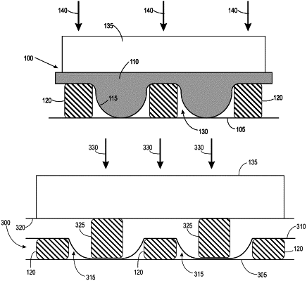
1. A pressure-activated membrane switch, comprising:
an electrically-conductive membrane;
a compliant conductive material comprising an upper surface and an electrically-conductive inner surface, wherein contact between the electrically-conductive membrane and the electrically-conductive inner surface of the compliant material is configured to cause an electrical circuit, of which the switch is a part, to close; and
a plurality of spacers dispersed between the electrically-conductive membrane and the compliant conductive material,
wherein:
the electrically-conductive inner surface is positioned against an upper surface of one or more of the plurality of spacers,
the plurality of spacers are positioned and configured to form one or more gaps between the electrically-conductive membrane, the plurality of spacers, and the compliant conductive material, and
the compliant conductive material is configured to deform between at least one of the one or more gaps when pressure is applied against the upper surface of the compliant conductive material toward the upper surface of one or more of the plurality of spacers, causing the compliant conductive material to contact the electrically-conductive membrane.
|