| CPC H01G 4/1227 (2013.01) [H01G 4/248 (2013.01); H01G 4/30 (2013.01)] | 19 Claims |
|
1. A multilayer capacitor comprising:
a body including a plurality of dielectric layers and a plurality of internal electrodes laminated in a first direction with respective dielectric layers interposed therebetween; and
external electrodes formed on external surfaces of the body and connected to the internal electrodes,
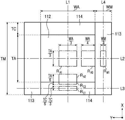
wherein the body includes an active portion, in which the plurality of internal electrodes are disposed to form capacitance, corresponding to a region between internal electrodes disposed on an outermost side in the first direction, among the plurality of internal electrodes, a cover portion covering the active portion in the first direction, and a side margin portion covering the active portion in a second direction, perpendicular to the first direction, and
wherein 1.49<A1/A2<2.50,
where A1 is an average grain size in a dielectric layer in the central region of the active portion, and A2 is an average grain size in a dielectric layer in an active-cover boundary portion, adjacent to the cover portion, of the active portion,
wherein 0.9<C2/M1<1.1,
where M1 is an average grain size in the central region of the side margin portion, and C2 is an average grain size in a dielectric layer in the cover-active boundary portion, adjacent to the active portion, of the cover portion.
|