| CPC G11C 8/06 (2013.01) [G06F 3/061 (2013.01); G06F 3/0659 (2013.01); G06F 3/0679 (2013.01); G11C 8/10 (2013.01)] | 17 Claims |
|
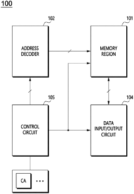
1. An address latch comprising:
a first address processing unit configured to latch external address signals to output first latched signals through an output node based on a read command and a write command; and
a second address processing unit configured to latch the external address signals based on the read command with a burst length that is set to a first value and configured to output second latched signals through the output node based on an internal read command.
|