| CPC G11C 7/222 (2013.01) [G11C 7/1057 (2013.01); G11C 7/1084 (2013.01)] | 19 Claims |

|
1. A semiconductor memory device comprising:
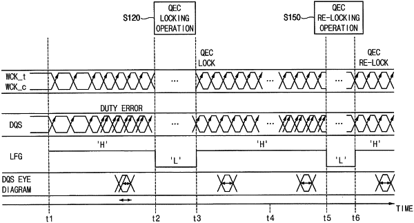
a quadrature error correction circuit configured to perform a relocking operation to lock a second corrected clock signal to a first corrected clock signal in response to a relock signal in a second operation mode, wherein the first corrected clock signal and the second corrected clock signal have a phase difference of 90 degrees with respect to each other and are generated based on first through fourth clock signals in a first operation mode;
a clock generation circuit configured to generate an output clock signal and a strobe signal based on the first corrected clock signal and the second corrected clock signal; and
a data input/output (I/O) buffer configured to generate a data signal by sampling data from a memory cell array based on the output clock signal and configured to transmit the data signal and the strobe signal to an external memory controller.
|