| CPC G11C 29/50004 (2013.01) [G11C 11/5628 (2013.01); G11C 16/12 (2013.01); G11C 29/021 (2013.01); G11C 29/023 (2013.01); G11C 29/028 (2013.01); G11C 29/42 (2013.01); G06F 3/0679 (2013.01); G06F 3/0688 (2013.01); G06F 11/1072 (2013.01); G11C 11/2275 (2013.01); G11C 13/0069 (2013.01); G11C 16/10 (2013.01); G11C 2029/5004 (2013.01)] | 20 Claims |
|
1. An apparatus comprising:
a memory cell array including a plurality of memory cells that include a first memory cell;
a word line connected to the plurality of memory cells; and
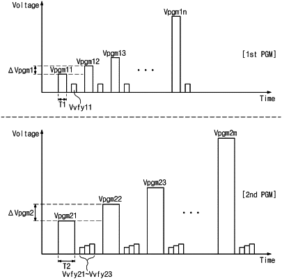
a controller configured to access the memory cell array, and configured to perform a first program operation on the plurality of memory cells to a first state among a plurality of states and then perform a second program operation on the plurality of memory cells to a second state among the plurality of states,
wherein for each of the plurality of memory cells, a first voltage level of the first state is less than a second voltage level of the second state,
the controller is configured to determine whether a program operation on the first memory cell to be performed is the first program operation or the second program operation,
when the controller determines that the program operation on the first memory cell to be performed is the second program operation, the controller is configured to adjust a programming voltage level for the first memory cell to the second voltage level and to program the first memory cell to the second state using the second voltage level,
the programming voltage level for the first memory cell is one of a plurality of programming voltage levels in the first and second program operations, and
a first programming voltage level of the plurality of programming voltage levels in the second program operation is less than a last programming voltage level of the plurality of programming voltage levels in the first program operation.
|