| CPC G11C 29/4401 (2013.01) [G11C 5/02 (2013.01); G11C 5/06 (2013.01); H01L 23/5384 (2013.01); H01L 23/5385 (2013.01); H01L 25/0657 (2013.01)] | 20 Claims |
|
1. An integrated circuit chip comprising:
a data node configured to conduct integrated circuit chip signals;
a first through electrode and a second through electrode, both electrodes being formed through the integrated circuit chip;
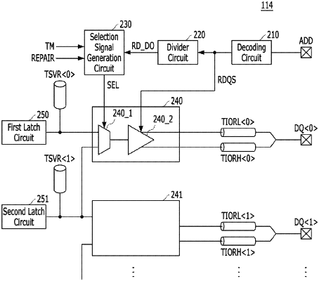
a transmission circuit comprising:
a selection signal input; and
a selector comprising: a first data input coupled to the first through electrode, a second data input coupled to the second through electrode and a data output;
the transmission circuit being configured to selectively couple, one of the first and second through electrodes to the data node, in response to a selection signal, provided to the selection signal input;
the integrated circuit chip additionally comprising:
a selection signal generation circuit, which is configured to provide the selection signal responsive to an active state of at least one of: a test operation signal, a repair signal and a read data strobe signal; and
a read driver configured to couple the selector data output to one of two different data lines in response to the read data strobe signal,
wherein the selection signal generation circuit comprises:
a first NAND gate suitable for receiving a repair information signal and a test mode signal and performing a NAND operation on the received signals;
a second NAND gate suitable for receiving the divided signal and an inverted signal of the repair information signal and performing a NAND operation on the received signals; and
a third NAND gate suitable for receiving output signals of the first and second NAND gates, and generating the selection signal by performing a NAND operation on the received signals.
|