US 12,009,042 B2
Executing a refresh operation in a memory sub-system
Vamsi Pavan Rayaprolu, Santa Clara, CA (US); Kishore Kumar Muchherla, San Jose, CA (US); Ashutosh Malshe, Fremont, CA (US); Gianni S. Alsasua, Rancho Cordova, CA (US); and Harish R. Singidi, Fremont, CA (US)
Assigned to Micron Technology, Inc., Boise, ID (US)
Filed by Micron Technology, Inc., Boise, ID (US)
Filed on Nov. 3, 2022, as Appl. No. 17/980,234.
Application 17/980,234 is a continuation of application No. 17/085,445, filed on Oct. 30, 2020, granted, now 11,521,699.
Prior Publication US 2023/0059923 A1, Feb. 23, 2023
This patent is subject to a terminal disclaimer.
Int. Cl. G06F 11/07 (2006.01); G06F 11/30 (2006.01); G06F 12/02 (2006.01); G06F 12/0882 (2016.01); G11C 29/10 (2006.01); G11C 29/42 (2006.01); G11C 29/44 (2006.01)
CPC G11C 29/42 (2013.01) [G06F 11/076 (2013.01); G06F 11/3037 (2013.01); G06F 12/0246 (2013.01); G06F 12/0882 (2013.01); G11C 29/10 (2013.01); G11C 29/44 (2013.01)] 20 Claims
OG exemplary drawing
 
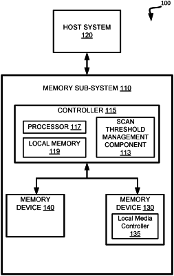
1. A method comprising:
executing a scan operation to identify a trigger rate associated with a set of memory pages of a data block of a memory device, wherein the trigger rate represents a number of the set of memory pages that fail an error management operation;
comparing the trigger rate to a threshold trigger rate to determine that a condition is satisfied; and
in response to satisfying the condition, executing, by a processing device, a refresh operation on the set of memory pages of the data block.