| CPC G11C 16/3459 (2013.01) [G11C 16/0483 (2013.01); G11C 16/08 (2013.01); G11C 16/10 (2013.01); G11C 16/14 (2013.01)] | 19 Claims |
|
1. A memory device, comprising:
a memory block including a plurality of pages coupled to a plurality of word lines, respectively;
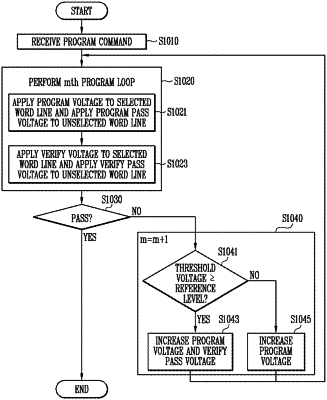
a peripheral circuit configured to perform a program loop including a program pulse operation of applying a program voltage to a selected word line corresponding to an address, among the plurality of word lines, and a verify operation of applying at least one verify voltage corresponding to the program voltage to the selected word line and applying a verify pass voltage to unselected word lines; and
control logic configured to:
control the peripheral circuit to repeatedly perform a next program loop including the program pulse operation and the verify operation until a pass signal indicating that the program pulse operation has passed according to the verify operation is received;
increase a level of the verify pass voltage applied to the unselected word lines whenever the peripheral circuit performs the next program loop when threshold voltages of memory cells included in a page coupled to the selected word line are greater than a reference level, wherein the unselected word lines include both word lines coupled to programed pages and word lines coupled to erased pages.
|