| CPC G11C 16/3459 (2013.01) [G11C 16/0433 (2013.01); G11C 16/0483 (2013.01); G11C 16/08 (2013.01); G11C 16/10 (2013.01); G11C 16/102 (2013.01); G11C 16/26 (2013.01); G11C 16/30 (2013.01); G11C 16/3404 (2013.01)] | 16 Claims |
|
1. A memory device, comprising:
memory strings each comprising a drain select gate (DSG) transistor and memory cells; and
a peripheral circuit coupled to the memory strings and configured to, in a program/verify cycle:
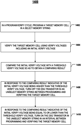
program a target memory cell of the memory cells in a select memory string of the memory strings;
after programming the target memory cell, verify the target memory cell using one or more verify voltages comprising an initial verify voltage;
compare the initial verify voltage with a threshold verify voltage so as to obtain a comparing result; and
control, at least based on the comparing result, the DSG transistor in an unselect memory string of the memory strings between programming and verifying the target memory cell,
wherein to control the DSG transistor, the peripheral circuit is further configured to, in the program/verify cycle, in response to the comparing result indicative of the initial verify voltage being equal to or lower than the threshold verify voltage, turn on the DSG transistor in the unselect memory string in an interval between an end of programming and a start of verifying the target memory cell, and
wherein the initial verify voltage is a maximum voltage of the one or more verify voltages.
|