| CPC G11C 16/0466 (2013.01) [G11C 16/10 (2013.01); G11C 16/16 (2013.01); G11C 16/26 (2013.01)] | 6 Claims |
|
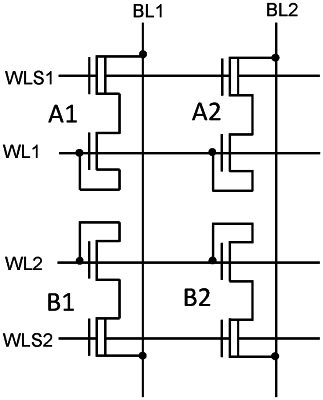
1. A memory array, wherein the memory array comprises:
a plurality of storage cells forming an array of M rows*N columns, each storage cell comprising a selection transistor and a memory transistor connected in series;
a plurality of bit lines arranged at intervals along the direction of columns, wherein drains of the memory transistors in the same column are connected to a corresponding bit line;
a plurality of memory transistor word lines arranged at intervals along the direction of rows; and
a plurality of selection transistor word lines arranged at intervals along the direction of rows, wherein the memory transistor word lines and the selection transistor word lines are arranged alternately, gates of the memory transistors in the same row are connected to a corresponding memory transistor word line, a source and a gate of each selection transistor are connected, the gates of the selection transistors in the same row are connected to a corresponding selection transistor word line, and all storage cells share a well region;
erasing, programming and reading of the storage cells are realized by applying certain voltage to the selection transistor word lines connected to the gates of the selection transistors, the memory transistor word lines connected to the gates of the memory transistors and the bit lines connected to the drains of the memory transistors.
|