| CPC G11C 11/419 (2013.01) [G11C 11/412 (2013.01); G11C 11/418 (2013.01)] | 19 Claims |
|
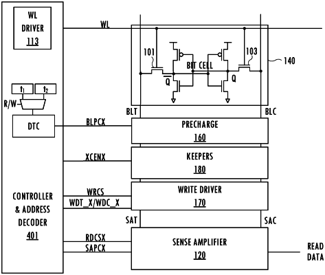
1. A method for accessing a memory cell, the method comprising:
enabling precharging of a bit line of the memory cell before a next access of the memory cell;
disabling the precharging after a first interval if the next access is a write; and
disabling the precharging after a second interval if the next access is a read, the first interval being shorter than the second interval,
wherein the bit line is precharged to a memory cell power supply voltage in response to the next access being a read or the next access being a write after a read access, and
wherein the bit line is precharged to a level less than the memory cell power supply voltage prior to a write column select signal cutting off the precharging of the bit line and driving a complementary bit line to ground in response to the next access being a write after a write access.
|