| CPC G11C 11/4076 (2013.01) [G11C 11/4096 (2013.01)] | 20 Claims |
|
1. A host system comprising:
a processor; and
a memory controller coupled to the processor, the memory controller to:
request a first reference voltage to be applied by memory devices;
during use of the first reference voltage by the memory devices:
transmit, to the memory devices, a chip select (CS) signal after various delay amounts and
receive, from the memory devices, samples of the CS signal transmitted after the various delay amounts;
request a second reference voltage to be applied by the memory devices;
during use of the second reference voltage by the memory devices:
transmit, to the memory devices, the CS signal after various delay amounts; and
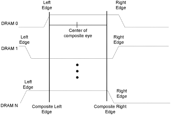
receive, from the memory devices, samples of the CS signal transmitted after the various delay amounts, wherein the processor is to determine a reference voltage for the memory devices based on the first and second reference voltages that provides a composite eye width that is closest to a reference eye width and determine a delay to transmit a subsequent CS signal based on the composite eye width.
|