| CPC G09G 3/3677 (2013.01) [G06F 3/0418 (2013.01); G06F 3/0443 (2019.05); G02F 1/13338 (2013.01); G02F 1/1368 (2013.01); G06F 3/044 (2013.01); G09G 2310/0286 (2013.01); G09G 2310/08 (2013.01); G09G 2320/103 (2013.01)] | 6 Claims |
|
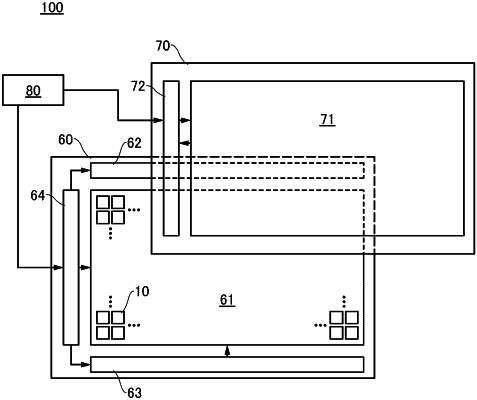
1. A display device comprising:
a display unit, the display unit comprising:
a touch sensor;
a pixel array;
a source driver electrically connected to a first demultiplexer; and
a plurality of gate drivers sandwiching the pixel array, one of the plurality of gate drivers comprising a first shift register,
wherein the first shift register comprises:
a first transistor, a second transistor, a third transistor, a fourth transistor, a fifth transistor, a sixth transistor, a seventh transistor, and an eighth transistor; and
a first wiring, a second wiring, a third wiring, a fourth wiring, and a fifth wiring,
wherein the first demultiplexer comprises a ninth transistor comprising silicon in a channel formation region,
wherein one of a source and a drain of the first transistor is electrically connected to the second wiring,
wherein the other of the source and the drain of the first transistor is electrically connected to the first wiring,
wherein one of a source and a drain of the second transistor is electrically connected to the other of the source and the drain of the first transistor, the first wiring, and one electrode of a first capacitor,
wherein a gate of the first transistor is electrically connected to the other electrode of the first capacitor and one of a source and a drain of the third transistor,
wherein a gate of the third transistor is electrically connected to the third wiring,
wherein the other of the source and the drain of the second transistor is electrically connected to the fourth wiring, one of a source and a drain of the eighth transistor, one of a source and a drain of the sixth transistor, and one electrode of a second capacitor,
wherein a gate of the fourth transistor is electrically connected to the fifth wiring,
wherein one of a source and a drain of the fourth transistor is electrically connected to one of a source and a drain of the seventh transistor, a gate of the fifth transistor, and a gate of the sixth transistor,
wherein one of a source and a drain of the fifth transistor is electrically connected to the other of the source and the drain of the sixth transistor, and
wherein the other of the source and the drain of the seventh transistor is electrically connected to the other of the source and the drain of the eighth transistor.
|