| CPC G09G 3/3648 (2013.01) [G11C 19/28 (2013.01); G09G 2310/0286 (2013.01)] | 10 Claims |
|
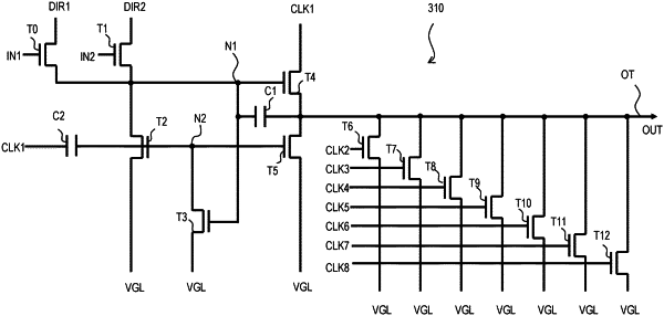
1. A display device, comprising:
a plurality of pixel circuit rows;
a plurality of selection lines connected to the plurality of pixel circuit rows; and
a shift register including a plurality of linked shift register units,
wherein the plurality of shift register units output sequential selection pulses to the plurality of selection lines,
wherein each of the plurality of shift register units outputs one of the selection pulses to a corresponding selection line among the plurality of selection lines,
wherein each of the shift register units includes a plurality of thin film transistors of a first conductivity type that are connected in parallel, and that, during an ON state, connect the corresponding selection lines to a fixed potential wiring line for applying a non-selection level for the one of the selection pulses,
wherein, during each frame period, the plurality of thin film transistors are turned ON/OFF by clock signals in different phases, and
wherein the duty cycle of the ON period of each of the plurality of thin film transistors during each said frame period is 12.5% or less.
|