| CPC G09G 3/3275 (2013.01) [H10K 59/121 (2023.02); H10K 59/65 (2023.02); G09G 2300/0452 (2013.01); G09G 2300/0842 (2013.01); G09G 2320/0646 (2013.01); G09G 2320/0673 (2013.01); G09G 2360/16 (2013.01)] | 19 Claims |
|
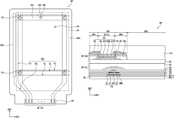
1. A display device, comprising:
a display panel including a first display area having a first light transmittance and a second display area having a second light transmittance higher than the first light transmittance; and
a driving controller configured to receive an image signal and to output a data signal for the display panel,
wherein the image signal comprises a first image signal corresponding to a first pixel unit in the first display area of the display panel and a second image signal corresponding to a second pixel unit and a non-pixel unit adjacent to the second pixel unit in the second display area of the display panel,
wherein the driving controller calculates a compensation signal based on a preset kernel matrix and the second image signal, and outputs a data signal corresponding to the second pixel unit in the second display area based on the compensation signal,
wherein the second pixel unit in the second display area of the display panel comprises:
a base layer;
a circuit element layer disposed on the base layer and including a shielding pattern;
a light emitting element disposed on the circuit element layer; and
an insulating layer disposed on the light emitting element,
wherein the non-pixel unit in the second display area of the display panel comprises the base layer and the insulating layer.
|