| CPC G09G 3/3233 (2013.01) [H01L 27/156 (2013.01); H01L 33/06 (2013.01); H01L 33/38 (2013.01); G09G 2300/0426 (2013.01); G09G 2300/0819 (2013.01); G09G 2300/0842 (2013.01); G09G 2310/0262 (2013.01); G09G 2310/08 (2013.01); G09G 2320/0233 (2013.01)] | 16 Claims |
|
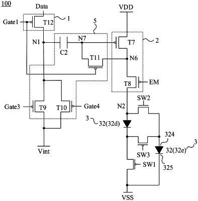
1. A pixel driving circuit, comprising:
a data writing circuit electrically connected to a first scanning signal terminal, a data signal terminal and a first node, the data writing circuit being configured to transmit a data signal received at the data signal terminal to the first node in response to a first scanning signal received at the first scanning signal terminal;
a light-emitting control circuit electrically connected to the first node, an enable signal terminal, a first voltage signal terminal and a second node, the light-emitting control circuit being configured to transmit a first voltage signal received at the first voltage signal terminal to the second node under control of a voltage of the first node and an enable signal transmitted by the enable signal terminal;
a first reset compensation circuit, and
a light-emitting diode chip electrically connected to the second node and a second voltage signal terminal, wherein
the light-emitting diode chip includes a plurality of light-emitting portions; the plurality of light-emitting portions include at least one first light-emitting portion and at least one second light-emitting portion;
a first bonding electrode of a first light-emitting portion in the at least one first light-emitting portion is electrically connected to the second node, and a second bonding electrode of the first light-emitting portion is electrically connected to the second voltage signal terminal;
a first bonding electrode of a second light-emitting portion in the at least one second light-emitting portion is electrically connected to the second voltage signal terminal, and a second bonding electrode of the second light-emitting portion is electrically connected to the second node;
the light-emitting diode chip is configured to, with cooperation of the first voltage signal from the second node and a second voltage signal received at the second voltage signal terminal, drive the plurality of light-emitting portions to emit light in different periods of time respectively or drive at least two light-emitting portions in the plurality of light-emitting portions to emit light in a same period of time;
wherein the light-emitting control circuit includes a first transistor and a second, transistor;
a control electrode of the first transistor is electrically connected to the enable signal terminal, a first electrode of the first transistor is electrically connected to the first voltage signal terminal, and a second electrode of the first transistor is electrically connected to a third node;
a control electrode of the second transistor is electrically connected to the first node, a first electrode of the second transistor is electrically connected to the third node, and a second electrode of the second transistor is electrically connected to the second node,
wherein the first reset compensation circuit is electrically connected to the first scanning signal terminal, a second scanning signal terminal, the first node, the second node, the third node and the second voltage signal terminal; and the first reset compensation circuit is configured to, under control of the first scanning signal and a second scanning signal received at the second scanning signal terminal, reset the pixel driving circuit and compensate for a threshold voltage of the second transistor;
the first reset compensation circuit includes a third transistor, a fourth transistor, a fifth transistor, a sixth transistor and a first capacitor;
a control electrode of the third transistor is electrically connected to the first scanning signal terminal, a first electrode of the third transistor is electrically connected to the second voltage signal terminal, and a second electrode of the third transistor is electrically connected to a fourth node;
a control electrode of the fourth transistor is electrically connected to the second scanning signal terminal, a first electrode of the fourth transistor is electrically connected to the third node, and a second electrode of the fourth transistor is electrically connected to a fifth node;
a control electrode of the fifth transistor is electrically connected to the second scanning signal terminal, a first electrode of the fifth transistor is electrically connected to the second node, and a second electrode of the fifth transistor is electrically connected to the fifth node;
a control electrode of the sixth transistor is electrically connected to the first scanning signal terminal, a first electrode of the sixth transistor is electrically connected to the fourth node, and a second electrode of the sixth transistor is electrically connected to the first node; and
a first terminal of the first capacitor is electrically connected to the fourth node, and a second terminal of the first capacitor is electrically connected to the fifth node.
|