| CPC G09G 3/3233 (2013.01) [G09G 2300/0819 (2013.01); G09G 2300/0842 (2013.01); G09G 2310/08 (2013.01); G09G 2320/045 (2013.01)] | 18 Claims |
|
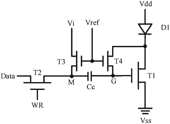
1. A pixel compensation circuit, comprising: a driving transistor, a data write-in transistor, a reset transistor, a compensation transistor, and a storage capacitor;
wherein a gate of the driving transistor is connected to a first node and a source of the driving transistor is connected to a negative electrode of a power source;
wherein a gate of the data write-in transistor is connected to a write-in signal input end, a source of the data write-in transistor is connected to a data signal input end, and a drain of the data write-in transistor is connected to a second node;
wherein a gate of the reset transistor is connected to a reset signal input end, a source of the reset transistor is connected to a reference signal input end, and a drain of the reset transistor is connected to the second node;
wherein a gate of the compensation transistor is connected to a reset signal input end, a source of the compensation transistor is connected to a positive electrode of the power source, and a drain of the compensation transistor is connected to the first node; and
wherein a first end of the storage capacitor is connected to the first node, and a second end of the storage capacitor is connected to the second node;
wherein during a first period, the reset transistor and the compensation transistor are turned on, the data write-in transistor is turned off, and the driving transistor is turned on;
wherein during a second period after the first period, the reset transistor and the compensation transistor are turned on, the data write-in transistor is turned off, and the driving transistor is turned off;
wherein during a third period after the second period, the reset transistor, the compensation transistor, the data write-in transistor and the driving transistor are all turned off;
wherein during a fourth period after the third period, the driving transistor and the data write-in transistor are turned on, and the compensation transistor and the reset transistor are turned off;
wherein during a fifth period after the fourth period, the driving transistor is turned on, the data write-in transistor, the compensation transistor and the reset transistor are turned off; and
wherein during a sixth period after the fifth period, the driving transistor is turned on, the data write-in transistor, the compensation transistor and the reset transistor are turned off.
|