| CPC G09G 3/32 (2013.01) [G09G 2310/0216 (2013.01); G09G 2310/0267 (2013.01); G09G 2330/028 (2013.01)] | 29 Claims |
|
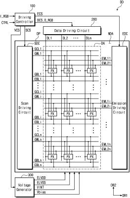
1. A pixel comprising:
a light-emitting element including an anode and a cathode;
a first transistor including a first electrode, a second electrode, and a gate electrode connected with a first node;
a third transistor connected between the second electrode of the first transistor and the first node and including a gate electrode connected with a first scan line;
a sixth transistor connected between the second electrode of the first transistor and the anode of the light-emitting element and including a gate electrode connected with a first emission line; and
a seventh transistor connected between the anode of the light-emitting element and an initialization voltage line and including a gate electrode connected with a second scan line,
wherein, during an initialization period, the third, sixth, and seventh transistors are turned on such that an initialization voltage from the initialization voltage line is transferred to the gate electrode of the first transistor.
|