| CPC G09G 3/22 (2013.01) [G06F 3/04166 (2019.05); G09G 3/32 (2013.01); G09G 2300/0426 (2013.01); G09G 2300/0819 (2013.01); G09G 2300/0852 (2013.01); G09G 2310/0202 (2013.01); G09G 2310/0267 (2013.01); G09G 2310/027 (2013.01); G09G 2310/08 (2013.01); G09G 2320/0247 (2013.01); G09G 2330/021 (2013.01); H10K 59/40 (2023.02)] | 20 Claims |

|
1. A pixel comprising:
a light emitting element;
a first transistor connected between a first power source and the light emitting element;
a second transistor connected between a data line and a first electrode of the first transistor, the second transistor including a gate electrode connected to a first scan line;
a third transistor connected between a gate electrode of the first transistor and a second electrode of the first transistor, the third transistor including a gate electrode connected to a second scan line;
a fourth transistor connected between the gate electrode of the first transistor and an initialization power source, the fourth transistor including a gate electrode connected to a third scan line; and
a storage capacitor connected between the first power source and the gate electrode of the first transistor,
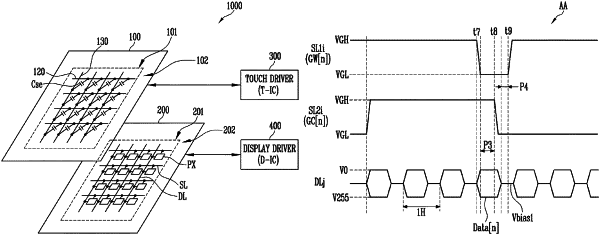
wherein a voltage provided through the data line is time divided into a data voltage provided to the gate electrode of the first transistor when both the second transistor and the third transistor are turned on, and an on-bias voltage provided to the first electrode of the first transistor when the second transistor is turned on and the third transistor is turned off,
wherein the second transistor is turned on by a first scan signal,
wherein the third transistor is turned on by a second scan signal, and
wherein a falling edge of the second scan signal is between a falling edge of the first scan signal and a rising edge of the first scan signal and overlaps a supply period of the first scan signal between the falling and rising edges of the first scan signal.
|