| CPC G09G 3/2092 (2013.01) [G09G 2310/0297 (2013.01); G09G 2310/061 (2013.01)] | 14 Claims |
|
1. A display panel comprising a plurality of rows and a plurality of columns of pixel circuits, a plurality of rows of gate lines, a plurality of rows of reset control lines, and a plurality of columns of data lines, wherein
a same row of pixel circuits corresponds to two rows of gate lines, and one row of gate line of the two rows of gate lines is electrically connected to odd-numbered columns of pixel circuits in the row of pixel circuits, and is configured to provide a corresponding gate driving signal for the odd-numbered columns of pixel circuits in the row of pixel circuits; the other row of gate line of the two rows of gate lines is electrically connected to even-numbered columns of pixel circuits in the row of pixel circuits, and is configured to provide a corresponding gate driving signal for the even-numbered columns of pixel circuits in the row of pixel circuits;
wherein the two rows of gate lines are only connected to the same row of pixel circuits, and not connected to another row of pixel circuits;
the same row of pixel circuits corresponds to a row of reset control line, and the reset control lines provide a corresponding reset control signal for the row of pixel circuits;
a same column of pixel circuits corresponds to two columns of data lines, and one column of data line of the two columns of data lines is electrically connected to odd-numbered rows of pixel circuits in the column of pixel circuits, and is configured to provide a corresponding data voltage for the odd-numbered rows of pixel circuits in the column of pixel circuits; and
the other column of data line of the two columns of data lines is electrically connected to even-numbered rows of pixel circuits in the column of pixel circuits, and is configured to provide a corresponding data voltage for the even-numbered row of pixel circuits in the column of pixel circuits,
wherein the two columns of data lines are only connected to the same column of pixel circuits, and not connected to another column of pixel circuits;
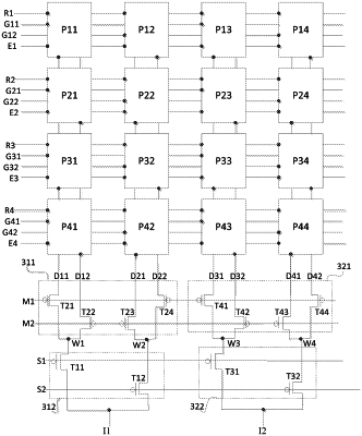
wherein the display panel further comprises a plurality of multiplexing circuits, wherein
the multiplexing circuit is configured to control a data voltage provided by a p-th data input terminal to be input to four columns of data lines in a time-division manner under the control of a multiplexing control signal provided by a multiplexing control line;
p is a positive integer;
wherein the multiplexing control line comprises a first multiplexing control line, a second multiplexing control line, a first column gate control line, and a second column gate control line;
a p-th multiplexing circuit comprises a p-th row of multiplexing sub-circuit and a p-th column of multiplexing sub-circuit;
the p-th column of multiplexing sub-circuit is respectively electrically connected to the p-th data input terminal, the first column gate control line, the second column gate control line, a (2p−1)th writing-in node and a 2p-th writing-in node, configured for controlling to connect or disconnect the p-th data input terminal and the (2p−1)th writing-in node, and connect or disconnect the p-th data input terminal and the 2p-th writing-in node under the control of the first column gate control signal provided by the first column gate control line and the second column gate control signal provided by the second column gate control line;
the p-th row of multiplexing sub-circuit is electrically respectively connected to the (2p−1)th writing-in node, the 2p-th writing-in node, the first multiplexing control line, the second multiplexing control line, the first column of data line, the second column of data line, the third column of data line and the fourth column of data line, and configured for controlling the (2p−1)th writing-in node to connect to the first column of data line or the second column of data line, and the 2p-th writing-in node to connect to the third column of data line or the fourth column of data line under the control of the first multiplexing control signal provided by the first multiplexing control line and the second multiplexing control signal provided by the second multiplexing control line; and
wherein the p-th row of multiplexing sub-circuit comprises a p-th first row of multiplexing transistor, a p-th second row of multiplexing transistor, a p-th third row of multiplexing transistor, and a p-th fourth row of multiplexing transistor,
a control electrode of the p-th first row of multiplexing transistor is electrically connected to the first multiplexing control line, and a first electrode of the p-th first row of multiplexing transistor is electrically connected to the (2p−1)th writing-in node, a second electrode of the p-th first row of multiplexing transistor is electrically connected to the first column of data line;
a control electrode of the p-th second row of multiplexing transistors is electrically connected to the second multiplexing control line, and a first electrode of the p-th second row of multiplexing transistors is electrically connected to the (2p−1)th writing-in node, a second electrode of the p-th second row of multiplexing transistor is electrically connected to the second column of data line;
a control electrode of the p-th third row of multiplexing transistors is electrically connected to the second multiplexing control line, and a first electrode of the p-th third row of multiplexing transistor is electrically connected to the 2p-th writing-in node, a second electrode of the p-th third row of multiplexing transistor is electrically connected to the third column of data line;
a control electrode of the p-th fourth row of multiplexing transistors is electrically connected to the first multiplexing control line, and a first electrode of the p-th fourth row of multiplexing transistors is electrically connected to the 2p-th writing-in node, a second electrode of the p-th fourth row of multiplexing transistor is electrically connected to the fourth column of data line.
|