| CPC G09G 3/20 (2013.01) [H03K 17/6872 (2013.01); G09G 2300/0819 (2013.01); G09G 2300/0852 (2013.01); G09G 2310/0267 (2013.01); G09G 2310/0286 (2013.01); G09G 2310/08 (2013.01); G09G 2330/021 (2013.01)] | 20 Claims |
|
1. A display panel comprising:
a pixel circuit comprising a writing transistor for controlling input of a data signal and a compensation transistor for controlling input of the data signal to a gate of a drive transistor; and
a gate drive circuit comprising a plurality of cascaded gate drive units, wherein each of the gate drive units comprises:
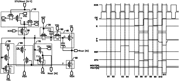
a stage transmission signal selection circuit electrically connected between a first wiring and a first node;
a pull-up control circuit configured to control a potential of a second node based on a potential of the first node and a potential of a first clock signal;
a pulse number reduction circuit electrically connected between the second node and a third node, the pulse number reduction circuit having a control terminal electrically connected to a reset line;
a first inversion circuit connected between the second node and a fourth node;
a first output stage configured to output a first gate control signal based on a potential of the third node and a potential of the fourth node; and
a second output stage configured to output a second gate control signal based on the potential of the second node,
wherein a number of pulses of the second gate control signal in one frame is greater than a number of pulses of the first gate control signal in one frame,
at least one of the stage transmission signal selection circuit, the first inversion circuit or the second output stage comprises three transistors with a same channel type, and
the first output stage has an output terminal electrically connected to a gate of the writing transistor, and the second output stage has an output terminal electrically connected to a gate of the compensation transistor.
|