| CPC G09G 3/006 (2013.01) [G09G 3/32 (2013.01); G09G 2330/12 (2013.01); H01L 22/32 (2013.01)] | 20 Claims |
|
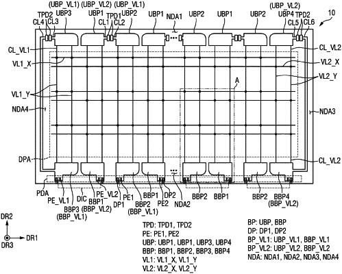
1. A display device comprising:
a display area and a first non-display area located on a side of the display area in a first direction;
a first bus pattern disposed in the first non-display area;
a second bus pattern disposed in the first non-display area and spaced apart from the first bus pattern in a second direction intersecting the first direction;
first voltage lines disposed in the display area, extending in the first direction, and electrically connected to the first bus pattern;
second voltage lines disposed in the display area, extending in the first direction, and electrically connected to the second bus pattern; and
a first test pad disposed in the first non-display area and disposed between the first bus pattern and the second bus pattern.
|