US 12,008,930 B2
Display panel and manufacturing method thereof
Yang Zhang, Wuhan (CN)
Assigned to WUHAN CHINA STAR OPTOELECTRONICS TECHNOLOGY CO., LTD., Wuhan (CN); and WUHAN CHINA STAR OPTOELECTRONICS SEMICONDUCTOR DISPLAY TECHNOLOGY CO., LTD., Wuhan (CN)
Appl. No. 17/434,723
Filed by WUHAN CHINA STAR OPTOELECTRONICS TECHNOLOGY CO., LTD., Wuhan (CN); and WUHAN CHINA STAR OPTOELECTRONICS SEMICONDUCTOR DISPLAY TECHNOLOGY CO., LTD., Wuhan (CN)
PCT Filed Jun. 8, 2021, PCT No. PCT/CN2021/098963
§ 371(c)(1), (2) Date Aug. 27, 2021,
PCT Pub. No. WO2022/236904, PCT Pub. Date Nov. 17, 2022.
Claims priority of application No. 202110500590.4 (CN), filed on May 8, 2021.
Prior Publication US 2024/0021112 A1, Jan. 18, 2024
Int. Cl. G06F 1/16 (2006.01); G09F 9/30 (2006.01)
CPC G09F 9/301 (2013.01) 20 Claims
OG exemplary drawing
 
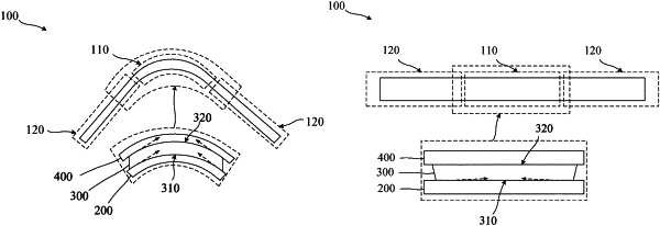
1. A display panel, comprising:
a first folding region; and
two non-folding regions located at two sides of the first folding region;
wherein the first folding region is provided with a first film layer, a second film layer, and a bonding layer between the first film layer and the second film layer;
wherein the bonding layer comprises a first surface in contact with the first film layer and a second surface in contact with the second film layer; and when the display panel is in a bent state, first tangential forces of the first film layer exerted on the first surface and second tangential forces of the second film layer exerted on the second surface point to a center of the first folding region.